Tuesday October 24, 2023, 8:30am
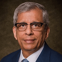
Dr. Waguih S. Ishak
Division VP & Chief Technologist, Silicon Valley
Corning Research & Development Corporation
Sunnyvale, CA
Presentation Title: Glass is a Key Material for the Connected World
Abstract: We are living a highly creative era in which digital consumer electronics will drive much of high-technology research and products for the betterment of people, society, and the environment. High speed communications, artificial intelligence, autonomous cars, AR/VR, quantum computing are just examples of what glass technology can make a big impact.
Biography: Dr. Waguih Ishak is the Division VP and Chief Technologist for Corning Research & Development Corporation. He joined Corning in 2007 to establish a new Silicon Valley facility, the Corning West Technology Center (CWTC) in Palo Alto, California. CWTC was chartered to build strong relationships with high-tech industries and academia in Silicon Valley and grew to conduct advanced research on optical interconnects, novel displays, and semiconductor devices & sensors. The Center moved to Sunnyvale in 2017 and is now called Corning Technology Center – Silicon Valley (CTCSV). Ishak grew the Center and built collaborative and joint research program with other entities in Corning applying glass and ceramic materials to semiconductor IC packaging, interposers, and AR/VR.
From 2005 to 2007, Ishak was the Chief Technology Officer and Vice President of Avago Technologies (now Broadcom) where he established the US R&D Center to do state of the art research in high speed semiconductors, semiconductor photonics and III-V compound semiconductor devices. From 2003 to 2005, Ishak was the Vice President and Director of the Photonics & Electronics Research Lab at Agilent Labs responsible for R&D programs in photonics, high-speed electronic ICs, semiconductor sensors, semiconductor tests, wireless communications and consumer electronics. From 1987 to 2003, Ishak was the Director of the Communications & Optics Research Laboratory at Hewlett-Packard Labs, working on photonics and integrated electronics. From 1978 to 1987, Ishak was a Scientist/Project Manager for bubble memories, SAW devices and MSW devices.
Ishak has authored approximately 100 journal and conference papers, and four chapters in the Handbook of Electronic Instruments. He was named an inventor on seven U.S. patents. He is on the technical advisory boards of USC, UCSDS, SCU, UCSB, and McMaster University. He was a member of the National Academics Committee on “Harnessing the Light” to write the book “Optics & Photonics – Essential Technologies for Our Nation,” 2013, resulting in the White House announcement of the Integrated Photonics Manufacturing Institute on October 2014. In 2016, Ishak was selected a member of the Visiting Committee on Advanced Technologies (VCAT) of the National Institute of Standards and Technology and served for 6 years from 2017 to 2022.
Ishak received a B.S.E.E. (hon.) from Cairo University in 1971 and a B.S. in mathematics (hon.) from Ain Shams University, Egypt, in 1973. He obtained his M.S. and Ph.D., both in electrical engineering, from McMaster University, Canada, in 1975 and 1978, respectively. Ishak obtained the Stanford University Executive Program in 1999 and was awarded a Doctor of Science honoris causa from McMaster University in 2018. Ishak is a Life Fellow of the IEEE, a Fellow of the Canadian Academy of Engineering, a member of the National Academy of Engineering, and received the University of California Exemplary Service Award in 2015.
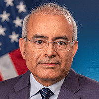
Yogendra Joshi
Program Manager
DARPA, Microsystems Technology Office
Arlington, VA
Presentation Title:Three Decades of Microsystems Thermal Management Research at DARPA
Abstract: DARPA's interest in thermal management of microsystems spans over three decades. A summary of past programs with a strong thermal management focus, and an overview of ongoing, and forthcoming thermal management initiatives will be presented. These programs have had a strong impact on the progress of high performance computing, and radio frequency systems. Past DARPA programs have often been followed by continuing research and development efforts by the performer communities, often resulting in new thermal technology breakthroughs. A recurring theme, along with successful transition of developed technologies into actual commercial products, has been the continuing focus on helping enable the highest performance microsystems. Emerging focus areas of interest including three-dimensional heterogeneously integrated microsystems, and microsystems for harsh environments will also be described.
Biography: Dr. Yogendra Joshi joined DARPA in July 2022 as a program manager in the Microsystems Technology Office (MTO). He is a professor and the John M. McKenney and Warren D. Shiver Distinguished Chair at Georgia Institute of Technology's G.W. Woodruff School of Mechanical Engineering. In addition, he has a courtesy appointment at Georgia Tech/s School of Electrical and Computer Engineering. His research interests are in multi-scale thermal management.
Joshi is the author or co-author of more than 450 publications in this area, including more than 225 journal articles. He received his Bachelor of Technology in mechanical engineering from the Indian Institute of Technology (Kanpur) in 1979, Master of Science in mechanical engineering from the State University of New York at Buffalo in 1981, and doctorate in mechanical engineering and applied mechanics from the University of Pennsylvania in 1984. He has served as the principal investigator for multiple DARPA programs and for the Office of Naval Research-led Consortium for Optimally Resource-Secure Outposts. He also previously was site director for the National Science Foundation Industry/University Cooperative Research Center on Energy Efficient Electronic Systems.
Joshi is an elected fellow of the American Society of Mechanical Engineers (ASME), the American Association for the Advancement of Science, and IEEE. He's been recognized for his contributions through several awards, including the Inventor Recognition Award from the Semiconductor Research Corporation (2001), the IBM Faculty Award (2008), the IIT Kanpur Distinguished Alumnus Award (2011), the AIChE Donald Q. Kern Award (2018), and multiple honors from IEEE and ASME.

Dr. Peter de Bock
Program Director
Advanced Research Projects Agency-Energy (ARPA-E) for the US Department of Energy
Presentation Title: ARPA-E High Risk/High Reward Technology Programs in Heat Transfer and Electronics
Abstract: The Department of Energy Advanced Research Projects Agency – Energy (ARPA-E)’s mission is to support transformational high risk/high reward projects in the areas of emissions, energy efficiency and increase leadership in critical technologies. Deployment of renewables, electrified transportation and rise in computing and datacenters, amongst others have led to an increasing role of electronics and electrical systems in our energy supply, transport and demand portfolio.
Due to the variable nature of power produced by renewables, it is projected that in the future up to 80% of all energy will flow through one form of power electronics to be suited for end-use. ARPA-E has supported transformational power electronics, motors and thermal management projects through CIRCUITS, CABLES and ASCEND programs. These projects are focused the enablement of more efficient power conversion and electrified transportation of complex systems such as aircraft.
Additional areas of interest are the efficient thermal management of complex electronic systems such as Data Centers through the COOLERCHIPS program. By exploring differential approaches, it can be observed that if low thermal resistance heat rejection can be realized at relevant system cost and reliability, significant energy savings could be realized. The presentation will describe an overview of these programs and highlights of technology developments that are to provide a basis for a more energy efficient future.
Biography: Dr. Peter de Bock currently serves as Program Director at the Advanced Research Projects Agency-Energy (ARPA-E) for the US Department of Energy. At ARPA-E Dr. de Bock manages and supports over teams in zero-carbon hybrid aviation propulsion systems through the $63M ASCEND program and efficiency of cooling of Data Centers through the $42M COOLERCHIPS program.
Prior to joining ARPA-E, Dr. de Bock worked at GE Research as Principal Engineer ThermoSciences. Dr. de Bock is the former chair of ASME K-16 committee on Heat Transfer in Electronics equipment, ASME Fellow, AIAA member and holds 50+ patents and publications with over 1000 citations.
Dr. de Bock received his Ph.D. in Mechanical Engineering from the University of Cincinnati and holds MSc degrees from University of Twente in the Netherlands, and University of Warwick in the UK.
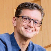
Christopher G. Malone, PhD, ASME Fellow
Meta
Presentation Title: Building a Global Gigawatt-Scale Data Center Fleet - Current and Future Challenges
Biography: Chris works with multi-disciplinary teams across Meta to develop integrated next-generation data center, hardware and software solutions and associated R&D investments. He supports the Meta sustainability teams on energy and carbon reduction technology investments.
Previously, Chris was a Distinguished Engineer at Google with responsibility for data center infrastructure design, technology strategy and R&D investments. He built and led teams covering chip packaging, IT hardware thermal solutions and data center power, cooling and systems architecture. He led the development of multiple generations of Google data center designs that have been deployed globally at the gigawatt scale.
Chris has authored numerous technical papers and has been granted over 100 patents. He is a co-author of the first paper on Power Usage Effectiveness (PUE), which has since become the industry standard data center efficiency metric. He is an ASME Fellow and was awarded the iMasons Industry Luminary award in 2022 for his contributions to the data center industry.
Chris received his MS and PhD in Mechanical Engineering from the Massachusetts Institute of Technology, Cambridge, MA, and the BEng (with Highest Honors) from Dalhousie University, Halifax, Nova Scotia.
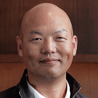
Vincent (WooPoung) Kim, Ph.D
Corporate EVP / Head of Advanced Packaging
SAMSUNG-DSRA
Presentation Title: Exciting work toward Advanced Packaging
Abstract: Heterogeneous Integration is highlighted as a key driver for the next era of Moore's law. By partitioning a large die into smaller chaplets and adopting an optimal process for each one, it significantly improves the overall yield and reduces manufacturing cost. Heterogeneous integration can also enhance the performance of chips by filling the gap between Logic performance and Memory bandwidth. With three-dimensional integration, in which one chip sits directly on top of another, signal paths can be reduced to several micrometer lengths, resulting in greatly improved latency. In addition, finer interconnect pitch in 3D integration enables extremely high bandwidth and memory density, resulting in higher performance.
This talk will share Samsung's exciting work toward Advanced Package with a specific focus on Specialized Memory Integration.
Biography: Dr. KIM is currently working as Corporate EVP / Head of DSRA-AVP in San Jose, CA. SAMSUNG has launched a new business unit to support the need of the semiconductor industry's advanced packaging for high-performance systems. The name of the new business is AVP (Advanced Packaging). Prior to joining Samsung, he was system architect for Signal Integrity and Power Integrity at Apple, path-finding for leading-edge consumer computers. Previously, he was with Qualcomm as SI manager in Snapdragon packaging. Earlier than Qualcomm, he was with Wireless Business Unit of Texas Instruments as co-design engineer optimizing the electrical design of OMAP packages/systems. Before TI, he was with Rambus as SI engineer to design and analyze memory systems. Dr. Kim received Ph.D Degree in ECE at Georgia Tech in 2004 and M.S. & B.A. degrees from KAIST, Korea in 1999 and 1997.
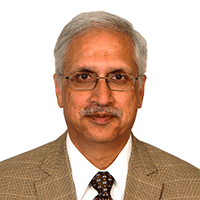
Sumanta Acharya
Program Director, Thermal Transport Processes (TTP)
National Science Foundation
Presentation Title: Thermal Management of Electronics: Research Supported by the National Science Foundation
Abstract: Thermal management of electronics is an active area of research in the thermal transport community. With increasing packaging density of power electronics, target cooling goals of 1KW/cm2 to 2KW/cm2 and avoidance of localized hot spots are desired. A range of cooling strategies with single-phase cooling, two-phase cooling with boiling (phase change), impingement cooling, and thin film evaporation among others are being explored. Related areas of active research include the role and control of surface morphology to promote phase change and high heat transfer coefficients, reducing the thermal resistance at the chip interface using high conductance thermal interface materials (TIM), and replacing Silicon by materials with higher conductivity and carrier mobility (such as diamond). The body of literature in these and related fields is extensive.
The Thermal Transport Processes (TTP) program at the National Science Foundation (NSF) has been supporting electronics cooling research for several decades. The focus of the research supported by NSF is motivated by the need for transformational scientific discoveries with potential for broad impact in the field. This talk will review the spectrum of research supported by NSF on electronics cooling and will highlight some key achievements. Future program interests and topics in this area will be discussed and ideas sought from the community.
Biography: Dr. Sumanta Acharya is currently the Program Director of the Thermal Transport Processes (TTP) program at the National Science Foundation (2022-present) and a Professor in the Department of Mechanical, Materials, and Aerospace Engineering at the Illinois Institute of Technology (IIT) in Chicago. From 2016 to 2022 he was also the Chair of Mechanical, Materials, and Aerospace Engineering, IIT Chicago.
Dr. Acharya's primary area of research is in computational and experimental thermal-fluid sciences. In recognition of his research, he was awarded the ASME Heat Transfer Memorial Award in the Science category, the AIChE Donald Q Kern Award, and the AIAA Thermophysics Award. Dr. Acharya He was previously the Chair of the ASME Heat Transfer Division. He is a Fellow of the ASME (American Society of Mechanical Engineers) and ASTFE (American Society of Thermal and Fluids Engineers) and Assoc. Fellow of AIAA (American Institute of Aeronautics and Astronautics).
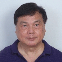
John H. Lau
Senior Special Project Assistant
Unimicron Technology Corporation
Presentation Title: Chiplet Design and Heterogeneous Integration Packaging
Abstract: Chiplet is a chip design method and heterogeneous integration is a chip packaging method. Chiplet design and heterogeneous integration packaging have been generated lots of tractions lately. For the next few years, we will see more implementations of a higher level of Chiplet designs and heterogeneous integration packaging, whether it is for cost, time-to-market, performance, form factor, or power consumption. In this lecture, the following topics will be covered.
- System-on-Chip (SoC)
- Why Chiplet Design?
- Chiplet Design and Heterogeneous Integration Packaging
- Chip partition and Heterogeneous Integration
- Chip split and Heterogeneous Integration
- Advantages and Disadvantages
- Lateral Communication between Chiplets (e.g., Bridges)
- Bridge Embedded in Build-up Package Substrate
- Bridge Embedded in Fan-Out EMC with RDLs
- UCIe
- Hybrid Bonding Bridge
- Chiplet Design and Heterogeneous Integration Packaging - Multiple System and Heterogeneous Integration
- Multiple System and Heterogeneous Integration with Package Substrate (2D IC Integration)
- Multiple System and Heterogeneous Integration with Thin Film layer on the Package Substrate (2.1D IC Integration)
- Multiple System and Heterogeneous Integration with TSV-less (Organic) Interposer (2.3D IC Integration)
- Multiple System and Heterogeneous Integration with Passive TSV-Interposer (2.5D IC Integration)
- Multiple System and Heterogeneous Integration with Active TSV-Interposer (3D IC Integration)
- Summary
- Potential R&D Topics in Chiplet Design and Heterogeneous Integration Packaging
Biography: John H Lau, with more than 40 years of R&D and manufacturing experience in semiconductor packaging, has published more than 515 peer-reviewed papers (375 are the principal investigator), 40 issued and pending US patents (25 are the principal inventor), and 23 textbooks (all are the first author). John is an elected IEEE fellow, IMAPS Fellow, and ASME Fellow and has been actively participating in industry/academy/society meetings/conferences to contribute, learn, and share. He received many awards, e.g., the ASME Worcester Reed Warner Medal and the IEEE Components Packaging and Manufacturing Technology Field Award.